
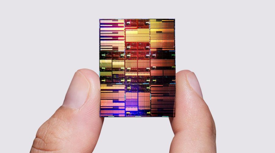
IBM Hails New ‘Block of Flats’ Design Breakthrough for Ultra Tiny Chips
IBM hails new block of flats – IBM has introduced a groundbreaking chip design that could revolutionize the semiconductor industry by enabling the placement of nearly 100 billion transistors on a chip as small as a fingernail. The company’s latest innovation, dubbed NanoStack, represents a significant leap in miniaturization, potentially achieving a size of 0.7 nanometres (nm)—a feat that could mark the first known chip technology to surpass the 1 nm threshold. This development comes at a pivotal moment as manufacturers face increasing challenges in scaling down components further while maintaining performance and efficiency.
The Quest for Smaller, Faster Chips
Traditionally, the standard chip size has been measured in nanometres, a unit that denotes a billionth of a meter. For years, the industry has adhered to a two-year doubling cycle for transistor counts, a principle famously known as Moore’s Law. However, as chips grow more complex, this trend has become harder to maintain. IBM’s new approach addresses this by shifting from horizontal scaling to a vertical design, stacking transistors in layers rather than spreading them across a single plane.
According to IBM, its prototype chip demonstrates a 50% performance improvement over its 2 nm technology and achieves 70% greater energy efficiency. This comes after the company unveiled its 2 nm chip in 2021, which already showed notable gains in processing speed and power consumption. The NanoStack design, however, promises even more dramatic advancements. By compressing transistors into a three-dimensional structure, IBM aims to overcome the physical limits of traditional manufacturing methods.
“With our new NanoStack architecture, we’re not just making smaller transistors, we’re reinventing how chips are built to deliver dramatically more power and energy efficiency,” said Jay Gambetta, director of IBM Research and IBM Fellow.
Challenges of 3D Chip Design
Despite the potential benefits, 3D chip fabrication introduces new complexities. One major hurdle is heat management: as transistors become denser, they generate more heat, which can impair performance and longevity. Additionally, when layers are too thin, transistors may fail to switch off properly, leading to operational inefficiencies. These issues require innovative solutions to ensure stability and reliability in ultra-tiny chips.
Professor Alan Woodward of Surrey University provided an apt analogy to illustrate the significance of IBM’s approach. He likened the NanoStack design to constructing a “block of flats” rather than individual houses in a city. “IBM’s NanoStack is like proposing a 100-storey skyscraper,” he remarked, contrasting it with competitors such as Samsung and Intel, which are currently working on 3D chips resembling 30- to 50-storey buildings. This comparison highlights the ambitious scale of IBM’s vision for future computing.
“I think it’s fair to say IBM’s proposals are the most ambitious,” said Prof Woodward, emphasizing the transformative potential of the technology.
The Role of Transistors in Modern Technology
Transistors, the fundamental building blocks of silicon chips, are critical to the functionality of electronic devices. They power everything from smartphones and gaming consoles to laptops and the vast data centres that process digital activities like streaming video and online banking. Moreover, their role has expanded with the rise of generative AI, which relies heavily on high-performance computing to deliver advanced capabilities.
As transistor density increases, so does the computational power of chips. This means devices can perform more tasks simultaneously, leading to faster processing and smarter features. However, achieving such density requires overcoming physical constraints. IBM’s NanoStack design seeks to do this by stacking layers of transistors, allowing for a denser configuration without increasing the chip’s footprint. This could pave the way for smaller, more powerful devices in the future.
Moore’s Law and the Future of Chip Manufacturing
Moore’s Law, which has guided the semiconductor industry for decades, is now being tested as manufacturers push the boundaries of miniaturization. While the law has held true for many years, experts acknowledge that its pace cannot continue indefinitely. The shift to 3D architecture, as IBM is pioneering, is a response to this challenge, aiming to maintain growth in performance and efficiency despite the limitations of traditional 2D fabrication.
IBM’s breakthrough is particularly noteworthy because it operates at a scale smaller than the current 2 nm standard. The 0.7 nm design not only reduces the physical size of chips but also enhances their capabilities. This could have far-reaching implications for industries reliant on advanced computing, such as healthcare, finance, and artificial intelligence. However, the technology is still in the prototype stage, with production readiness expected to take several years.
As the demand for faster, more efficient electronics grows, innovations like NanoStack are essential. They enable devices to handle complex tasks while maintaining compact form factors. This is especially important for portable gadgets and wearable technology, where size and power consumption are critical factors. IBM’s work represents a bold step forward in meeting these demands.
Outside the UK, readers can subscribe to the Tech Decoded newsletter to stay updated on the latest advancements in technology. The article also references recent developments in quantum computing and AI chip design, underscoring the dynamic nature of the field. These innovations collectively signal a new era of technological progress, driven by the relentless pursuit of miniaturization and efficiency.
With its NanoStack design, IBM has set a new benchmark for chip manufacturing. By reimagining the structure of transistors, the company aims to deliver unparalleled performance and energy savings. While challenges remain, this breakthrough could redefine the capabilities of modern electronics and lay the foundation for the next generation of computing devices.